The concept of the CCD was described by Boyle and Smith [1970] as:
Basically, it consists of storing charge in potential wells created at the surface of a semiconductor and moving the charge (representing information) over the surface by moving the potential minima... In particular, we consider minority carrier charge storage at the Si-SiO2 interface of a MOS capacitor.
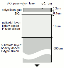
Figure 4.2: The MOS structure
of a surface channel CCD
detector showing "typical" dimensions.
Subsequent testing by Amelio et al. [1970] showed that Boyle’s concept was valid. Although the structure of a modern CCD detector differs in a number of ways from these initial devices, which are called surface channel devices, the basic principals of operation remain. Based on a survey of available literature, the MOS structure of a "typical" surface channel CCD detector is illustrated in Figure 4.2. In practice the CCD will be divided into individual picture elements called pixels with each of these pixels consisting of up to four of these MOS structures.
In order for a CCD to function as an optical detector, it must be capable of converting the photons arriving at it’s surface into an electrical signal. For descriptive purposes, the operation of a CCD detector is broken into 4 simple steps which are discussed in following sections.
Step 1: Charge Generation
The generation of charge in a CCD detector is done by the photoelectric effect. On exposure to light a certain number of photons will be absorbed in the epitaxial layer of the CCD (see Figure 4.2) resulting in an electronhole pair. The quantum efficiency of the CCD can then be defined as the ratio of the number of electron-hole pairs generated to the number of photons incident at the surface of the CCD. Note that it is only those electron-hole pairs generated within the epitaxial layer that contribute to the detected signal.
The basic structure of the CCD in combination with the optical properties of silicon have significant effects on the variation of the quantum efficiency with wavelength.
- The large refractive index of silicon results in a significant amount of light being reflected from both surfaces of the gate as well as from the epitaxial layer. Interference fringes are often observed. Anti-reflection coatings, either on to or instead of the silicon dioxide passivation layer, will reduce the fringing caused by internal reflections within the gate region but have little impact on the throughput of light into the epitaxial layer. Consequently there is little improvement of the quantum efficiency.
- At short wavelengths the absorption depth in silicon is sufficiently small that nearly all the photons are absorbed in the gate area and will therefore not contribute the detected signal. The quantum efficiency is usually negligible at wavelengths less than 400nm.
- As the wavelength is increased the absorption depth also increases rapidly with the result that larger numbers of photons will completely pass through the epitaxial layer and not contribute to the detected signal. Photons with energies less than the band-gap energy will not be absorbed at all. For silicon this corresponds to wavelengths greater than 1100nm.
Using the structure described (Figure 4.2), the quantum efficiency can be modelled using standard thin-film techniques. The theoretical efficiency, illustrated in Figure 4.3, has the same general features as the quantum efficiency of real devices such as the SITe SI-003A (frontside illuminated).
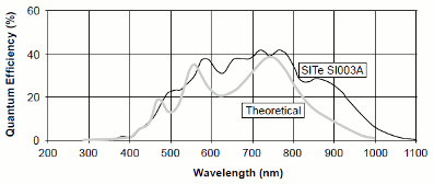
Figure 4.3: Quantum efficiency of a frontside illuminated CCD.
Improving the Blue Response
The poor blue response of the basic CCD is largely due to the absorption of photons in the gate area. Ideally the gates should have both high electrical conductivity and low optical absorption, however although materials other than silicon have been tried, fabrication and reliability difficulties mean that no viable alternative has yet been found. Fortunately there are other methods that may be employed to improve the CCD’s response to shorter wavelengths:
- Fluorescent Dye Coating
- Certain organic dyes such as corene or lumogen absorb photons in the UV and blue region of the spectrum and reemit at longer wavelengths. By coating the surface of a CCD with such a dye, effective quantum efficiencies of between 10 to 20% can be achieved at shorter wavelengths. In other regions of the spectrum, the dyes are non-absorbing and have little effect.
- Backside Illumination - Thinning
- A more direct approach to the problem is to avoid having the photons pass through the gates. In a process commonly referred to as thinning, the CCD chip is first chemically etched to remove the substrate layer below the imaging area and then mounted with the gate structure against a rigid support. Incident photons, arriving on the etched ”rear” surface do not pass through the gate electrodes at all. Once enhancement and anti-reflection layers are applied, significant increases in quantum efficiencies at all wavelengths are possible.
- Virtual Phase
- Developed by Texas Instruments for use in it’s own CCDs, virtual-phase technology [Hynecek, 1981] provides devices with high blue response by removing one of the gates from a 2-phase (2 gates per pixel) CCD. Although not as effective as backside illumination, simplified fabrication means that Texas Instruments’ virtual phase CCDs are no more expensive than standard devices.
For comparison purposes the theoretical quantum efficiencies of these enhancement techniques are shown in Figure 4.4. The effectiveness of backside illumination is also illustrated by the manufacturer’s data for the SI-003A CCD [Sci, 1996] in Figure 4.5.
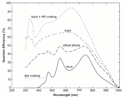
Figure 4.4: Quantum efficiencies of blue enhanced CCDs.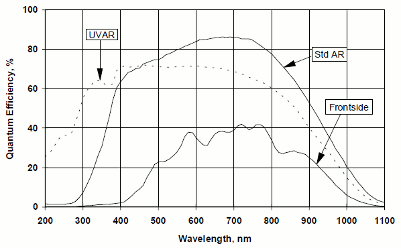
Figure 4.5: SITe SI-003A CCD quantum efficiency.
Dark Current
Unfortunately electron-hole pairs are also randomly generated in the silicon due to natural thermal processes. Although indistinguishable from photoelectrically generated charges, the rate at which the "thermal" charges are generated (dark current) is strongly temperature dependant. Practical values follow the well known Boltzmann law (Equation 4.1) with the dark current being reduced by a factor of approximately two for every 7K drop in temperature.
![]() - (Eqn 4.1)
- (Eqn 4.1)
At room temperature the dark current limits the maximum exposure time to about one or two seconds, therefore cooling of the CCD detector is required for the long exposure times often required in the astronomical application of CCDs.
Step 2: Charge Collection
Unlike single element sensors where the effect of arriving photons can be monitored directly, in the case of area detectors it is necessary to integrate over a period of time. This is equivalent to the "exposure time" for photographic films. In the case of CCDs it is photoelectrically generated charge that must be accumulated
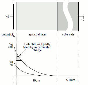
Figure 4.6: Surface channel
MOS potential well.
Consider the basic MOS structure in Figure 4.6 with the gate held at a positive potential with respect to the substrate. The electric field will cause holes in the lightly doped P-type epitaxial layer to diffuse down into the substrate leaving part of the epitaxial layer depleted of charge carriers. If electron-hole pairs are generated in or near this region, either photoelectrically or thermally, then the electrons will diffuse to the region at the Si-SiO2 boundary where the local electrostatic potential is most positive. Here they are collected as signal. The holes on the other hand will diffuse down into the substrate where they are effectively lost.
The simplest pixel, consisting of three adjacent MOS structures with the middle gate held at a more positive potential than the outer gates, defines the region where the local electrostatic potential is most positive and is the region of minimum potential energy for the electrons. The capacity, or depth, of this potential well depends mainly on the applied potentials on the MOS gates and on the pixel dimensions. The well depth is defined as the maximum number of electrons that may be accumulated with well depths ranging from about 50,000 electrons to as many as 500,000 under normal operating conditions. Should this number be exceeded then charge will "leak" into adjacent areas, an effect commonly referred to as blooming.
Various techniques for draining away excess charge, not surprisingly known as anti-blooming, have been developed by manufacturers primarily for the video applications of CCDs. The use of anti-blooming, however, usually results in a reduction in performance, such as reduced well depth and sometimes poorer linearity. For these reasons anti-blooming is rarely used in scientific applications. Details of the anti-blooming technique used by Texas Instruments is described in detail by Hynecek [1983].