In any system, detection or otherwise, there are performance limiting factors which determine the range of signal levels over which the system is useful. At very small signal levels there is always a random uncertainty to the exact signal level – noise. Over a large range of signal levels the system’s output may not be directly proportional to the input – linearity or distortion. Together these two factors determine the useful range of signal levels – dynamic range.
Noise
In a CCD system there are a number of sources contributing to uncertainty in the detected output. The uncertainty, or noise, can take a number of forms however it is only the time-variant types that will be considered here. Uncertainties that are time-invariant (or close to it), such as pixel to pixel variations and quantising errors, can often be measured and compensated for. Following is a brief discussion on the main sources of noise.
- Due to the time-random nature of charge generation, either photoelectrically or thermally, the uncertainty in the total charge detected is equal to the square root of the total. Other events, such as cosmic rays, will also contribute. The contribution from the statistics of photon arrivals is of course inherent in all light detection systems and is a property of the source rather than the detector. The thermal component can be dramatically reduced by cooling the CCD and cosmic ray events can be detected and removed by comparison of two or more exposures of the same field.
- The charge detection circuits also contribute noise. Consider first the RC combination represented by the reset switch, S, and capacitance, C, shown in the diagram. When the switch is closed the capacitor, C, rapidly charges up to the reference voltage, and simultaneously comes into thermodynamic equilibrium with the variance in the energy stored on the capacitor being given by the classical equipartition theorem as ½q²/C = ½kT. The charge stored fluctuates about a mean value with a standard deviation of √(kTC) and the standard deviation in the voltage, that is the RMS reset noise is √(kT/C) This reset noise, expressed as electron equivalents, can be in the order of hundreds of electrons.
When the reset switch is subsequently opened the very high resistance represented by the switch will result in a long relaxation time (very limited bandwidth). Provided the two samples of the output signal are taken on a time scale much shorter than the relaxation time then the noise is effectively frozen and is removed subsequent signal processing. It will therefore contribute little to the detected signal.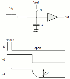
- The dominant source of noise generated within the CCD is the output amplifier whose purpose is to isolate and buffer the potential on the charge detection capacitor. This circuit consists of one or more field effect transistors (FETs) which contribute both white noise, consisting of a combination of thermal and shot noise, and 1/f noise which is due to the trapping of charge carriers at the surface of the conductive channel within the FET [see Soclof, 1985, chapter 14 for details].
The amount of noise at the output pin of the CCD detector, or read noise, is specified by the white noise, as a mean-squared voltage per unit bandwidth, and the 1/f noise corner frequency, fn, at which the 1/f noise power becomes equal to the white noise power. Many manufacturers quote the noise in terms of electron equivalents for a recommended set of operating conditions. Improvements in fabrication methods have resulted in the noise being reduced from the 10 to 20 electrons found in early devices to as little as 1 or 2 electrons. - There are also numerous other sources of noise which may effect the performance of a CCD camera system. These include feedthrough noise from the clocking signals, errors caused by jitter in the clock timing, white and 1/f noise from signal processing circuits. Interference caused by external sources such as power distribution lines (50 or 60 Hz) and electrical/electronic equipment, especially computers, can also have significant effects if adequate precautions are not taken.
Clearly the overall noise performance of a CCD system depends on a large number of factors, however in terms of detecting the charge from a given pixel, it is primarily the read noise which determines the uncertainty. In a well designed CCD system sources of noise external to the CCD detector, including interference, will cause only minimal degradation of the overall performance.
Non-linearity
The ideal transfer function for a CCD, that is the ratio of the signal output to the number of photons in, is a straight line between "zero" and "saturation". Non-linearity is a measure of by how much the actual transfer function deviates from this ideal case and is often defined as the peak deviation as a percentage of the overall range. It may also be convenient to quote the non-linearity over a smaller range, for example from 0% to 60% of the well depth. Typical values for CCDs are in the order of 1%.
Sometimes the transfer function is defined in terms of its gamma (γ), where
![]() - (Eqn 4.2)
- (Eqn 4.2)
For CCDs γ is nearly always in the range 0.9 to 1.0.
Although small, non-linearity is a measurable parameter affecting the overall performance of a CCD detector system. Unfortunately, however, available literature provides little enlightenment on the actual cause of these non-linearities. After considering the operating principles behind the CCD detector, I would suggest the following causes of non-linearities in CCDs. The relative merits of each are dependant on, amongst other things, the physical structure of the CCD detector in question.
- During the process of charge accumulation in a pixel, the electric field causes photoelectrically (or thermally) generated electrons diffuse to the potential well. As the potential well fills, charge from the accumulated electrons counteracts the electric field and the width of the depletion region becomes smaller. These facts suggest that, as the potential well fills, an increasing number of electrons are not accumulated and thus the overall quantum efficiency of the CCD effectively falls. Non-linearities caused in this manner would be more pronounced at longer wavelengths because these photons will generate electrons deeper within the silicon.
- The energy levels of electrons accumulated in a potential well follow a distribution due to thermal or other processes. As the well’s capacity is approached, there is a statistically increasing portion of the electrons that have enough energy to escape the potential well and "tunnel" into adjacent areas such as neighbouring pixels. If the energy distribution is primarily thermal in nature (just like dark current), then these non-linearities would exhibit a strong temperature dependance. The use of anti-blooming techniques to stop electrons from tunneling into adjacent pixels generally has causes a noticeable degradation of linearity.
- The ultimate form of non-linearity is saturation, or the point where the well’s capacity has been reached. This can be defined as the equilibrium condition where the number of electrons diffusing into the well equals the number tunneling out. Saturation can also occur in other regions, such as the serial register if the charge from multiple pixels is combined (a process called binning).
- Finally we need to convert the charge to a potential by transferring it onto a small capacitance. The assumption that the capacitance is constant, and therefore that the "detection" process is linear, is not necessarily true. One method of creating such capacitance is to use a reverse-biased P-N junction where the "signal" end of the capacitor is an area of N-type silicon in the P-type substrate. Because the N-type region is normally at, or near, the positive reference potential, a depletion region will form resulting in capacitance. Unfortunately the width of the depletion region, and hence the capacitance, is a function of the potential and will be modulated by the signal voltage. Real CCDs are somewhat more advanced that this simplified model suggests, however non-linearities due to such effects will still occur albeit at very low levels.
Although the CCD represents a significant improvement in performance over most other forms of detector, non-linearities do exist and may need to be accounted for in precision quantitative applications.
Bibliography
- G.F. Amelio, M.F. Tompsett, and G.E. Smith
- Experimental verification of the charge coupled device concept. Bell System Technical Journal, (49):593, 1970.
- W.S. Boyle and G.E. Smith
- Charge coupled semiconductor devices. Bell System Technical Journal, (49):587, 1970.
- C.F. Claver, M.E. Cornell, and C.B. Opal
- Evaluation of the texas instruments tc215-31 ccd for astronomical imaging. In Instrumentation in Astronomy VII, volume 1235 of SPIE Proceedings, 1990.
- J. Hynecek
- Virtual phase technology: A new approach to fabrication of large area ccds. IEEE Transactions on Electron Devices, ED-28(5):483–489, May 1981.
- J. Hynecek
- Electron-hole recombination antiblooming for virtual-phase ccd imager. IEEE Transactions on Electron Devices, ED-30(8):941–948, August 1983.
- Scientific Imaging Technologies
- SITe 2048 X 4096 Scientific-Grade CCD - Data Sheet, 1994.
- Scientific Imaging Technologies
- SITe 1024 X 1024 Scientific-Grade CCD - Data Sheet, 1996.
- Texas Instruments
- TC215 1024 X 1024 Pixel CCD Image Sensor - Data Sheet, 1991.
- R.H. Walden et al
- The buried channel charge coupled device. Bell System Technical Journal, (51):1635, 1972.